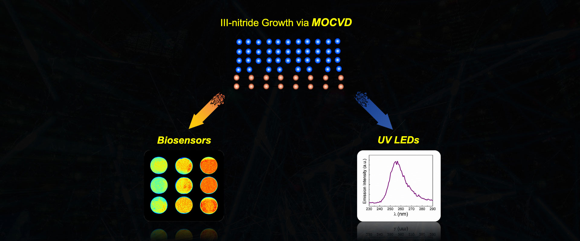
Our research efforts are driven by the desire to improve human lives through innovated technologies with III-nitride compound semiconductors. Specifically, metal-organic chemical vapor deposition (MOCVD) is used to produce the III-nitride wafers, whose unique optical and electrical properties are utilized to design and fabricate next-generation optoelectronic devices. Research projects are in close collaboration with the industries, and often requires multidisciplinary specialties. Current studies are focused on two major areas:
Surface-enhanced Raman spectroscopy (SERS) is one of the most powerful biosensing techniques. The technique is not only highly sensitive, but also capable of delivering label-free, real-time and multiplex detection of target molecules. However, SERS biosensors nowadays are still rarely found in practical applications. The main culprit is reliability. In Lai group, we address the issue by nanostructured InGaN quantum wells, which greatly expand the SERS-active regions, thus improving the spatial and temporal reliability of SRES signals. The quantum wells have been found effective in SERS sensing of DNA and other analytes. We hope these promising results can advance relevant biomolecular studies and the development of clinical diagnostics.
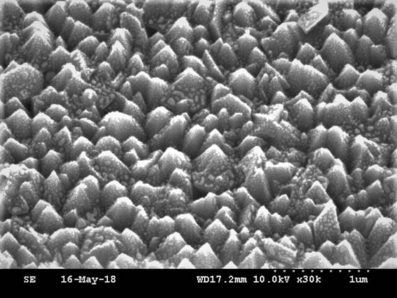
Ultraviolet (UV) light emitting diodes (LEDs) have grabbed increasing markets in curing industries, disinfection and many other applications. These market promises are fueled by the advantages of the solid-state emitter, including small size, low power consumption, and long lifetime. Although the compact light source is commercially attractive, quantum efficiencies of AlGaN-based UV LEDs, particular for the wavelength below 300 nm, are still much lower than those of their InGaN-based counterparts. The Lai group has developed several unique growth tactics for high-quality AlN epitaxial layer, which is the essential material for UV emitters. New materials are also under investigation with the attempt to further push device performances. We aim to benefit the industry by providing a feasible and cost-effective manufacturing techniques for deep UV LEDs.
Copyright @ 2018 LAI RESEARCH GROUP. All Right Reserved.